ZESTRON’s Impact on Semiconductor Manufacturing and Reliability
ZESTRON provides precision cleaning chemistries, surface conditioning solutions, process development and analytical services for semiconductor manufacturing. Across power electronics, advanced packaging and wafer-level applications, we help manufacturers establish controlled surface conditions for soldering, sintering, wire bonding, underfill and encapsulation. Chemistry selection and process parameters are tailored to the target residues, exposed materials, equipment and downstream requirements, with compatibility and performance verified through application-specific testing.
Explore our three application areas. Each connects surface preparation to a defined manufacturing step and measurable qualification outcome:
1. Power Electronics 2. Advanced Packaging 3. Wafers

Effective surface preparation combines contaminant removal with controlled rinsing, drying and handling.
Where required, surface conditioning adjusts oxide state, surface chemistry or wettability to prepare interfaces for subsequent processing. These controls matter because organic films can obstruct bond formation or create weak interfacial layers, particles can prevent intimate contact, and mobile ionic contaminants can promote leakage, corrosion and electrochemical migration under moisture and electrical bias. ZESTRON connects residue analysis and surface characterization with process optimization and downstream qualification to help manufacturers achieve repeatable surface preparation for reliable bonding and encapsulation
Semiconductor applications across industry segments
AI/HPC, military and aerospace electronics, e-mobility and other semiconductor applications rely on different combinations of computing, sensing, communication and power conversion. Their packaging and wafer processes create distinct cleaning and surface preparation requirements. The table below connects these applications to the interfaces that require control.
| Industry Segment | Representative Semiconductor Applications | Surface Preparation Priorities |
|---|---|---|
| AI and HPC infrastructure | GPU and accelerator chiplets; HBM; network switches; optical engines; power conversion | Large-package residue transport; dense interconnects; bond-ready surfaces; thermal interfaces |
| Military defense and aerospace | RF and mixed-signal SiP; radar and communications electronics; onboard computing | Bond and seal interfaces; ionic contamination; traceability; mission-specific environmental qualification |
| E mobility and transportation | SiC traction modules; onboard chargers; DC–DC converters; charging infrastructure; ADAS compute | Sinter and solder interfaces; mold adhesion; humidity bias and insulation robustness |
| Industrial and energy systems | Motor drives; robotics; photovoltaic inverters; storage converters; grid power electronics | Corrosion control; durable die attach; high-voltage interfaces and repeatable processing |
| Communications and photonics | Data-center optical engines; telecom RF devices; PIC and EIC assemblies | Optical and electrical compatibility; particles; coatings and adhesive interfaces |
| Medical and connected devices | Imaging and sensing ICs; compact diagnostic modules; wearable SiP | Low leakage; bond and encapsulation integrity; compatibility with sensitive structures |
1. Power Electronics
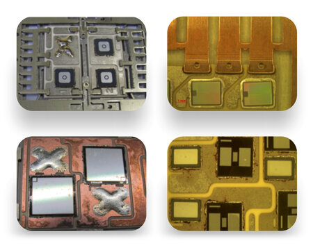
Surface preparation for high voltage and high power density packages
Power packages combine semiconductor dies, metallized substrates, bonding layers, interconnects and encapsulants. Their reliability depends on the interfaces between these materials under electrical, thermal and mechanical stress. SiC and GaN enable demanding power-conversion designs, but the package must still manage heat flow, insulation and thermomechanical loading.
Applications and material stacks
-
Applications include e-mobility traction inverters, onboard chargers, fast charging, renewable-energy conversion, industrial drives and AI infrastructure power supplies. Relevant devices include silicon IGBTs and MOSFETs, SiC MOSFETs and diodes, and GaN power transistors. GaN RF devices also support communications and defense applications; their RF packaging requirements differ from those of GaN power switching devices.
Typical assembly materials include copper leadframes, direct bonded copper (DBC) and active metal brazed (AMB) ceramic substrates, Ag- or Ni-based finishes, solder, sinter materials and mold compounds. DBC and AMB are substrate constructions, not semiconductor devices. Compatibility must be assessed across the complete exposed stack, including ceramic edges, barrier layers and passivation.
Preparation before solder and sinter attachment
-
Organic films, particles and uncontrolled oxides can interfere with wetting or bonding. For solder attachment, preparation should promote consistent wetting while preserving metallization. For sintering, it should establish the surface condition required by the selected paste and finish. Deoxidation must control metal loss, surface roughness and reoxidation during transfer.
A representative development sequence is residue characterization, compatible cleaning or conditioning, controlled rinse and dry, defined storage or transfer, bonding, and inspection of the resulting joint. The exact sequence depends on whether the bonding system uses a flux, reducing atmosphere, pressure or a pre-applied material. Avoid adding a treatment that leaves an interlayer incompatible with the joint.
Ag and Cu sintering
-
Pressure-assisted and pressureless sintering are distinct process options. Paste formulation, surface finish, die size and atmosphere determine the applicable process window. Copper-based systems need careful oxide and oxygen management; silver-based systems also require compatibility and residue control rather than an assumption of surface tolerance. Both pressureless and pressure-assisted Cu sinter applications have commercially been used in recent times.
Power Electronics Cleaning Challenges and Surface Readiness
Why residue removal becomes difficult
Soldering and sintering expose organic materials to heat, changing their solubility and leaving deposits with different chemical and physical properties. Flux spatter can reach wire-bond pads and adjacent ceramic or metal surfaces. Clips, stepped substrates, multiple bonding surfaces and narrow clearances restrict fluid exchange. An accessible outer surface can look clean while deposits remain in sheltered regions. Bonding and molding surfaces therefore require targeted inspection.
Removal strength must be balanced against selectivity. A treatment that dissolves a residue may also attack copper, thin plating, solder or exposed barrier layers. Mixed-metal assemblies can respond differently from single-metal coupons. pH alone does not predict compatibility: the complete formulation, temperature, exposure and rinse conditions matter.
Why a clean and conditioned surface is essential
|
Residue or surface condition |
Potential consequence at the next step |
Required process objective |
|---|---|---|
|
Organic films on bond or mold surfaces |
Block intimate contact or form a weak boundary layer; contribute to low bond strength or delamination |
Remove interfering films before bonding or molding; verify adhesion on the selected material pair |
|
Unsuitable copper oxide or residual passivation |
Interfere with solder wetting or metallic contact in the selected bonding process |
Establish the specified oxide state without excessive metal loss; control reoxidation and staging time |
|
Accessible flux activators and ionic contamination |
With moisture and bias, it may contribute to leakage, corrosion, ECM or AMP |
Remove target ionic species and verify extraction recovery; test electrical behavior under relevant stress |
|
Cleaner carryover or retained moisture |
Introduce a new film or ionic source; interfere with encapsulation or subsequent thermal processing |
Qualify rinsing and drying before the interface is sealed |
Surface conditioning may be needed as part of cleaning process because the exposed metal or dielectric can remain chemically unsuitable for the next step. Conversely, a freshly deoxidized surface is not automatically ready for molding: the encapsulant chemistry, surface aging and any inhibitor residue must also be considered.
How to demonstrate the benefit
Compare the existing process with the proposed treatment using representative parts. Link residue and surface-state measurements to wire pull or die shear, failure location, mold adhesion, acoustic inspection and relevant humidity-bias or cycling results. A stronger bond at time zero does not by itself establish long-term insulation or interface reliability.

Power Electronics Bonding Technologies
Soldering, sintering, wire bonding and planar interconnects form different electrical, thermal and mechanical connections within power packages. Each requires preparation of its own bonding surfaces. Diffusion soldering in discrete devices and sintered module attachment illustrate why the selected metallurgy and process determine the preparation strategy.
|
Bonding Technology |
Technical Relevance |
Surface Preparation Requirement |
|---|---|---|
|
Solder die and substrate attach |
Liquid-phase wetting and intermetallic formation; fluxed or controlled-atmosphere variants |
Remove interfering films; preserve solderable finish; clean accessible flux residues where required |
|
Ag or Cu sinter attach |
Particle consolidation for die, substrate or heat-spreader attachment; pressure conditions depend on material |
Control organic and oxide state; prevent incompatible films; verify bond strength and failure location |
|
Diffusion soldering and transient liquid phase (TLP) bonding |
A liquid phase participates in forming a higher-melting joint; exact metallurgy determines conversion |
Control metallization and oxides; qualify reaction completion, bond phases and remaining residues |
|
Wire and ribbon bonding |
Al, Cu or Au systems with different ultrasonic, thermal and pad requirements |
Remove pad contamination; control oxide condition without damaging thin finishes or passivation |
|
Copper clip and planar interconnects |
Lower-profile current paths attached by solder, sinter or other qualified methods |
Prepare both bonding faces; account for blocked access after clip placement and multiple attach steps |
|
Double sided cooled structures |
Multiple bonding planes and exposed surfaces before encapsulation |
Develop staged cleaning and handling before interfaces are sealed; preserve existing joints and alignment |
Surface conditioning after sintering before molding
Post-sinter surface preparation addresses the exposed surfaces that will contact the mold compound or encapsulant. These surfaces may retain process-derived organic films or other contaminants even when the sintered joint meets its mechanical criteria. Removal and conditioning should preserve the die attach, bond pads, ceramic and metallization while preparing the intended adhesion interfaces.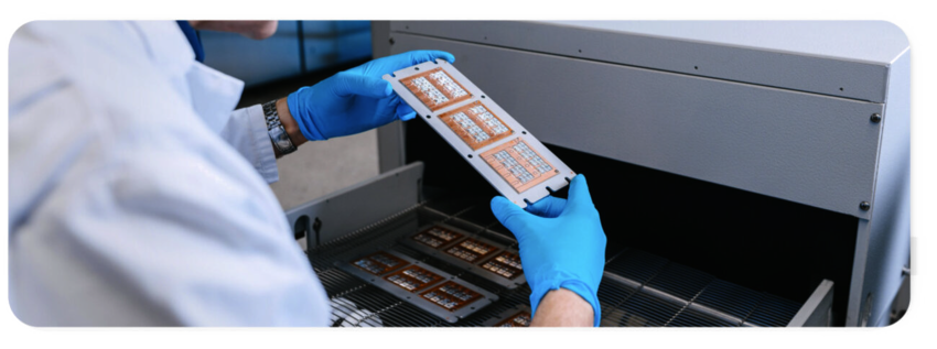
ZESTRON and MacDermid Alpha investigated post-sinter surface conditions on single- and double-sided cooled packages. This work addresses the interface between sintering and molding, where exposed substrate surfaces need preparation for the subsequent encapsulant. The treatment is evaluated against the actual sinter material, metallization and mold compound.
The objective is to ensure reproducible adhesion surface that complements the qualified sintering and molding processes. Evaluate mold adhesion on the treated material pair, including surface aging and the production interval between preparation and molding. This connects the surface treatment to the interface it is intended to improve.
Power Electronics Qualification and Process ControlAdhesion moisture and high voltage reliability
Weak adhesion and delamination can create pathways for moisture and alter electrical stress at interfaces. In the presence of susceptible metals and mobile ionic species, electrical bias can contribute to leakage and corrosion. High-voltage anodic migration phenomenon (AMP) requires mechanism-specific diagnosis and should not be equated with conventional ECM/dendritic growth. Package geometry, materials and operating environment remain part of the reliability assessment.
Surface conditioning should therefore be evaluated through both surface characterization and assembly performance. A lower contact angle alone does not prove stronger mold adhesion or better insulation. It is important to compare untreated controls and treated samples after representative environmental stress and document the observed failure mode.
|
Qualification objective |
Useful evidence |
Interpretation |
|---|---|---|
|
Residue removal |
Microscopy; FTIR for suitable organics; ion chromatography with controlled extraction, |
Identify and quantify the target residue; verify method recovery and blank contribution |
|
Oxide and surface chemistry |
SEM/EDX where needed; controlled contact-angle measurements |
Distinguish cleanliness, chemical state and wettability |
|
Bonding quality |
Die shear; wire pull or shear; cross sections; void and BLT (bond line thickness) assessment |
Assess strength, failure location and morphology; establish limits for the actual metallurgy |
|
Mold and encapsulant adhesion |
Adhesion tests; acoustic microscopy; post-aging delamination assessment |
Check the actual material pair and staging time; correlate interface changes with reliability |
|
Electrical and thermal durability |
Relevant humidity-bias testing; insulation tests; thermal or power cycling |
Match voltage, humidity and load conditions to the package mission and failure mechanism |

Qualification aligned to the product
Automotive discrete-device qualification and power-module qualification have different scopes. AEC-Q101 addresses discrete semiconductors; ECPE AQG 324 addresses automotive power modules. A cleaning chemistry is not itself “AEC-qualified,” and cleaning results do not establish module qualification. Use the applicable customer specifications, current document revision and agreed test plan.
How ZESTRON supports implementation. We support...
- Residue Identification
- Chemistry Screening
- Material Compatibility Trials
- Process Development
Concentration, temperature, exposure, rinse exchange, drying, bath loading and post-clean staging time should be controlled as an integrated process. Analytical results are linked to bonding and encapsulation outcomes rather than used as isolated pass/fail indicators.
Prepare critical interfaces for reliable bonding and encapsulation. Connect with ZESTRON’s application engineering team to develop and qualify cleaning and surface conditioning processes for die attach, and the post-sinter and pre-mold stages of power module assembly.
2. Advanced Packaging
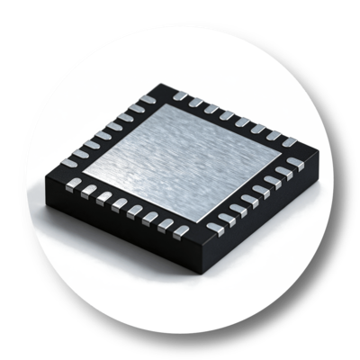 Surface readiness for chiplets memory stacks and heterogeneous integration
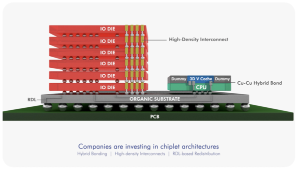
Advanced packaging integrates multiple functions within one package. Flip chip connects a face-down die through bumps; BGA provides external array connections; PoP stacks packages; and SiP combines dies and components.
AI/HPC uses chiplets and HBM, while military and aerospace electronics combine logic, RF and sensing. These architectures require reliable interfaces across dissimilar materials.
Bonding technologies require different contamination strategies
|
Technology |
Bond formation and integration role |
Cleaning and conditioning implication |
|---|---|---|
|
Mass reflow with solder bumps |
Immediate bonding for flip chip, BGA and selected stacked assemblies |
When flux is used, qualify residue removal and rinsing before underfill or encapsulation closes access |
|
Thermocompression bonding |
Local force and thermal cycle; may use flux, pre-applied underfill or nonconductive film / paste (NCF/NCP) |
Select preparation before bonding; a film or paste-filled interface cannot be cleaned like an open capillary gap |
|
Fluxless thermocompression bonding |
Oxide management through tool-specific reducing or activation processes |
May remove the flux-cleaning step at that interface; assess incoming contamination, tool chemistry and adjacent interfaces |
|
Laser assisted bonding or local reflow |
Localized energy delivery to form the selected joint |
The heat source does not define residue chemistry; assess flux use, thermal by-products, metallurgy and process access |
|
Cu to Cu direct metal bonding |
Metallic bonding without conventional solder; conditions depend on oxide state, microstructure, pressure and temperature |
Control organic films, oxidation, topography and recontamination; this is not a dielectric hybrid bonding process |
|
Dielectric and Cu to Cu hybrid bonding |
Direct bonding of dielectric surfaces with embedded metal interconnects |
Requires coordinated particle control, surface chemistry, planarity, copper recess, activation and handling |
Fluxless is a change in process requirements
It is a process that can avoid a conventional post-bond flux wash at the relevant interface. It does not remove the need to control particles, handling films, adhesive residues or other contamination elsewhere in the flow.
For formic-acid or plasma-assisted routes, it is important to investigate residual species or deposits when indicated by surface or process evidence. Do not assume tin formate, “tin fog” or another contaminant is present or absent solely because a process is fluxless. Select additional wet treatment only when it addresses an identified need without compromising the bonding surface.
Advanced Packaging: Hybrid Bonding and HBM
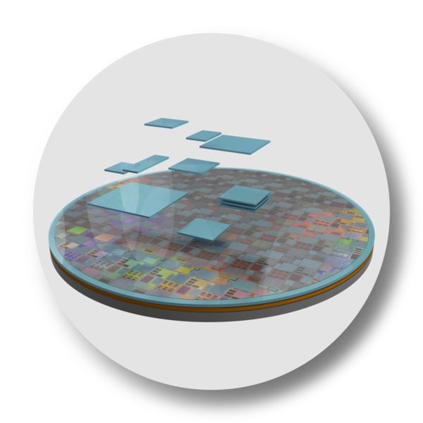
Wafer to wafer (W2W) and die to wafer (D2W) bonding
Wafer-to-wafer (W2W) bonding joins prepared wafers and is sensitive to die-layout compatibility, wafer-level yield and distortion. Die-to-wafer (D2W) bonding enables selection of known-good dies and integration of dissimilar die sizes, while adding singulation, handling and placement contamination risks. Both need coordinated preparation and alignment while their pitch and overlay capabilities are not interchangeable.
In a dielectric/Cu hybrid flow, CMP establishes the surface topography. Cleaning removes slurry-related particles and films; activation sets the required dielectric surface state; controlled handling maintains that state until contact and anneal. The actual sequence depends on the tool and material system. An oxide-removal treatment that is appropriate for exposed copper must also preserve the dielectric and required copper recess.
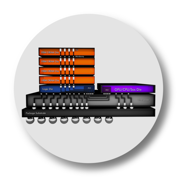
HBM microbumps underfill and stacking
High-bandwidth memory combines stacked DRAM, vertical interconnects and a base die. Mass reflow with molded underfill (MR-MUF), thermocompression with nonconductive film (TC-NCF) and emerging hybrid-bonded stacks use different bonding and encapsulation sequences.
For open microbump interfaces, characterize flux location and the access available before molding. For TC-NCF, preparation and material controls precede formation of the film-filled interface. For hybrid-bonded memory or logic stacks, particles and surface state replace flux removal as the central bond-interface preparation problem. The selected architecture determines where wet chemistry can contribute.
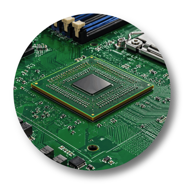
Large Form Factor Packages
Cleaning under a large fcBGA or interposer depends on gap geometry, bump obstruction, access length, residue solubility and fluid exchange. Wetting alone does not establish through-gap removal. As gaps narrow, replenishment and rinse displacement become increasingly difficult. It is recommended to use representative assemblies and destructive access on sacrificial samples to assess the region before underfill.
Advanced Packaging Copper Pillar InterconnectsTechnology and application relevance
Copper-pillar interconnects use plated copper posts, commonly with a solder cap, to connect a flipped die to a substrate, interposer or wafer. The copper post provides a less-collapsible structure than a solder-only bump; the solder cap forms the metallurgical joint in a soldered assembly. Pillar diameter, array pitch, solder volume and bonding conditions together influence joint geometry and the assembled die-to-substrate clearance.
These interconnects support dense I/O in compute, RF, SiP and heterogeneous packages. For AI/HPC chiplets and selected memory-integration flows, increasing connection density raises the need for controlled residue removal before underfill or molding. The cleaning strategy follows the actual flux, bonding and encapsulation sequence.

Gap height is different from pitch and pillar height
A gap below 25 µm refers here to the assembled clearance between opposing die and substrate surfaces that the cleaning fluid must access. Bump pitch is the lateral center-to-center spacing between interconnects; pillar height describes the copper feature before or within the assembled stack. Solder cap geometry, pads, passivation, local warpage and assembly conditions affect the available flow path.
Why copper pillar assemblies are difficult to clean
Flux used during solder attachment may remain around the joint, beneath the die or near passivation and solder-mask features. Reflow conditions or aging can change residue solubility. Dense arrays obstruct transport, while a large die footprint increases the distance to the center. Residue loading and trapped air can further restrict access. DI-water cleanability must therefore be demonstrated after the actual thermal cycle and on the actual geometry even in case of water-soluble tacky flux materials.
Surface compatibility is equally important. Appropriate chemistry must preserve exposed Cu, solder, barrier or finish layers, pads, passivation and substrate polymers. Extended exposure or excessive mechanical energy can improve flux removal while increasing metal loss or assembly damage. Compatibility trials should include representative patterned parts and aged cleaning baths, as appropriate.
Preparing the interface for underfill and encapsulation
Residual organic films can interfere with underfill wetting or form weak adhesion layers; particles can obstruct flow; and mobile ionic species may contribute to leakage or corrosion under moisture and bias. The objective is to achieve a clean, dry and chemically suitable interface before it becomes inaccessible. It is important to evaluate underfill flow, voids and adhesion using the chosen material combination.
ZESTRON supports copper-pillar defluxing through residue analysis, chemistry selection, compatibility testing and process development. Our published study describe DI-water and low-concentration cleaning-agent comparisons, followed by work on finer-pitch CoW (down to 10µm) devices. These provide a basis for evaluation and the customer geometry determines the qualified process window.
Advanced Packaging Cleaning Below 25 Micrometers
Developing a process for restricted gaps
For accessible gaps below 25µm, the challenge includes delivering fresh chemistry, dissolving residue, removing contaminated liquid, replacing it with rinse water and drying the interface. There is no single gap height that establishes cleanability. Die footprint, local minimum clearance, bump layout, residue chemistry and available flow paths all matter. ZESTRON’s low-standoff guidance describes trials in the 10–40 µm range and emphasizes component-size-to-gap relationships.
|
Process Requirement |
Technical Challenge |
Development and Verification Focus |
|---|---|---|
|
Wetting and access |
Trapped air and narrow channels can limit ingress into the central region |
Assess wetting and real access on the assembled geometry; low surface tension alone is insufficient |
|
Residue removal |
Reflowed residues may be slow to dissolve or poorly soluble in DI water |
Match chemistry to thermally processed residue; evaluate concentration, temperature and exposure together |
|
Fluid exchange |
Dense arrays and long paths restrict replenishment and removal of dissolved material |
Optimize equipment, orientation and dwell; assess local removal without excessive pressure or acoustic energy |
|
Rinsing and drying |
Cleaner, dissolved residues and water can remain beneath the die |
Qualify rinse displacement, carryover and drying before encapsulation; examine locations where fluid ingress is challenging |
|
Material and joint integrity |
Chemical attack and mechanical stresses can damage a successfully cleaned assembly |
Assess metal loss, passivation, joint condition and die integrity alongside cleaning performance |
Qualification before underfill
Use representative samples with the intended flux volume, reflow history, die size and minimum assembled gap. Inspect edge, intermediate and center regions using destructive access on sacrificial parts where needed. Include controls for any residue redistribution or damage introduced by opening the interface. Microscopy and targeted ionic or organic analysis should be matched to the contaminant and the sampling geometry.
Correlate cleanliness with underfill behavior, acoustic inspection for voids or delamination, adhesion and relevant electrical or environmental testing.
Connect with ZESTRON’s application engineering team to evaluate copper-pillar and sub-25 µm gap cleaning, including chemistry, equipment, rinsing, drying and readiness for underfill. Qualification is specific to the package and residue system; the gap dimension alone is not a guaranteed capability limit.
Advanced Packaging Cleaning Challenges and Interface Failures
Restricted access makes cleaning a transport problem
Fine-pitch bumps and low standoff reduce the open space available for flow. Large dies increase the distance that cleaning and rinse liquids must travel. Dense bump arrays, residue accumulation and trapped air can further restrict exchange. Fluid entering a gap is not evidence that fresh chemistry reaches every location or that dissolved material leaves the interface.
Successful removal requires wetting, dissolution, and transport away from the surface, rinse displacement and drying. A low-surface-tension formulation can assist access, but cannot compensate for insufficient residue solubility or fluid exchange. Increasing spray pressure, temperature, chemical exposure time or ultrasonic energy may introduce component damage, metal attack or delamination. It is important to optimize the entire process instead of focusing on a single parameter.
Why residue removal is critical
|
Interface |
Cleaning or preparation challenge |
Why the final surface matters |
|---|---|---|
|
Flip chip and capillary underfill |
Reflowed residues and trapped rinse beneath obstructed gaps |
Films can change underfill wetting and adhesion; residual ions may affect electrical behavior under moisture and bias |
|
HBM and stacked chiplets |
Access closes during stacking, bonding or molding |
Contamination sealed into an interface cannot be assumed removable by a subsequent wash |
|
Cu and dielectric hybrid bonding |
Particles, thin organic films and oxide/topography changes on prepared surfaces |
Particles can prevent local contact and generate bond voids; films or unsuitable Cu state can interrupt the intended bond |
|
Optical engines and CPO |
Electrical residues coexist with sensitive optical coatings and coupling regions |
Deposits can alter optical loss; an aggressive clean can damage the optical or adhesive interface |
For a fluxed reflow process followed by capillary underfill, it is important to perform required cleaning, rinsing, drying and verification before underfill dispense and cure. TC-NCF and other pre-applied encapsulant flows require upstream surface preparation and material controls instead of an assumed post-bond wash. A no-clean flux classification does not establish suitability for every underfill, optical assembly or customer reliability requirement.
Cleanliness and activation are separate requirements
Hybrid bonding needs both contaminant removal and the specified dielectric and metal surface condition. Plasma activation may modify the surface, while wet cleaning can remove selected residues and particles; neither replaces CMP topography control. Select and validate their sequence to avoid corrosion or recontamination. It is important to preserve the prepared state through dicing, handling and transfer.
Advanced Packaging Photonics and Large Area Integration
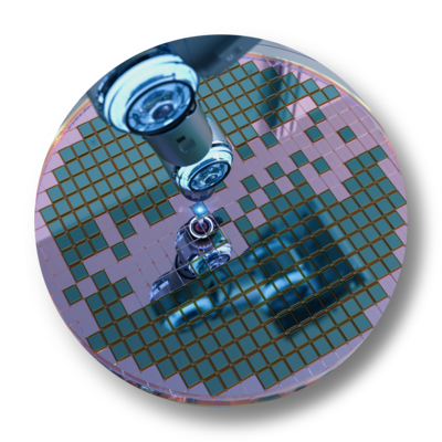
Silicon photonics and co-packaged optics
Photonic integrated circuits (PICs), electronic ICs, laser sources and fiber interfaces introduce multiple bonding and contamination requirements. Electrical connections may use solder or direct bonding, while optical assembly may use eutectic attachment, adhesives or other routes. It is important to treat electrical contact surfaces, optical coupling areas and coating or adhesive interfaces separately.
Particles and films near optical coupling regions can affect loss or alignment stability. Compatibility evaluation should cover exposed metallization, passivation, optical coatings, polymer structures and adhesives. Validate optical performance after cleaning and aging; electrical cleanliness alone is insufficient.
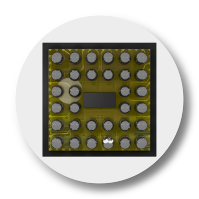
Glass Interposers
Interposers, bridges, redistribution layers and vertical stacks determine access, material exposure and the sequence in which interfaces close. A technology family can use more than one bonding approach.
Fan-out wafer-level (FOWLP) and fan-out panel-level (FOPLP) packaging introduce reconstituted substrates, molding materials and fine redistribution layers. Glass-core substrates and through-glass vias add different metal/glass and adhesion interfaces.
Process development should assess large-area uniformity, edge and backside contamination, panel or wafer distortion, exposed copper and polymer compatibility.
Qualification for compute defense and optical packages
|
Interface or application |
Evidence needed beyond visual cleaning |
|---|---|
|
Soldered chiplet or fcBGA attachment |
Localized residue analysis; rinse recovery; post-underfill void and adhesion checks; electrical testing |
|
Hybrid bond interface |
Particle mapping; surface chemistry; roughness and recess; overlay; bond voids and electrical continuity |
|
CPO and optical engine assembly |
Optical loss or coupling measurement; coating and adhesive compatibility; thermal alignment stability |
|
Military aerospace and harsh environments |
Program-defined shock, vibration, thermal and moisture tests; traceable lots; relevant microcircuit test methods |
Prepare silicon photonics and co-packaged optics assemblies for reliable electrical and optical performance. Connect with ZESTRON’s application engineering team to characterize contamination, evaluate cleaning effectiveness and material compatibility, and optimize surface preparation before bonding and encapsulation. Our application-specific trials help assess residue removal, adhesion and optical performance while protecting sensitive materials and interfaces.
3. Wafers
Residue removal and surface preparation for selected wafer level processes
Wafer bumping creates electrical attachment features; redistribution layers route connections; lithography uses patterned photoresist; and temporary carriers support thin wafers. These processes introduce different residues before subsequent bonding or coating steps. ZESTRON supports application-specific removal and surface preparation while evaluating compatibility with the exposed material stack.
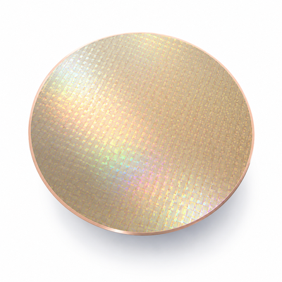 Wafer bumping copper pillars and redistribution layers
Electroplated solder bumps, Cu pillars with solder caps and redistribution layers involve lithography, plating and selected metal-removal steps. Photoresist fragments, plating-related organics, particles and post-reflow flux must be distinguished. Resist stripping, seed-layer etching, oxide treatment and defluxing have different objectives and selectivity requirements.
Post-bump reflow cleaning targets flux residues while protecting bump shape, under-bump metallization and passivation. It is important to select the product and process to ensure the residue is fully removed without impacting the exposed metals and wafer tool configuration..
Photoresist stripping and metal lift off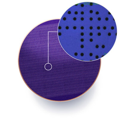
Resist chemistry, thickness, bake history and exposure to plating, plasma or other thermal processes affect dissolution and crosslinking. A stripper should remove the target film and fragments without excessive metal attack or damage to adjacent dielectrics and permanent polymers. Chemistries effective for thick packaging resist should not be assumed suitable for every front-end resist.
Metal lift-off removes a sacrificial resist with overlying unwanted metal. It is a different operation from etching a patterned metal layer. Fragment generation, metal flakes, redeposition and rinse transition become important to particle control.
Choosing organic aqueous and inorganic chemistry
Organic solvent systems may address selected polymeric residues and aqueous formulations may combine solvation, alkalinity, complexation or other functions. On the other hand, inorganic or reducing treatments may address specific oxide or surface-state requirements. Select chemistry from the contaminant and desired endpoint, then verify material compatibility and contamination introduced by the treatment itself.
Wafers Temporary Bonding and Thin Wafer Handling
Carrier release and post debond cleaning
Temporary carriers support thinning, backside processing and handling of fragile wafers. Thermal, mechanical, laser and other release methods act on different adhesive or release-layer systems. Separating the carrier and removing remaining material are distinct operations. The cleaning requirement follows the actual adhesive stack and its process history.
Residual adhesive can exist as a continuous film, localized islands, edge bead or thermally modified fragments. Dissolution, swelling and gel formation can produce different transport and redeposition behavior. It is important to evaluate removal rate and residual film rather than rely on disappearance of tack or bulk material alone.
A representative flow is carrier separation using the qualified release method, supported-wafer residue removal, controlled intermediate or final rinsing, drying and inspection, followed by the specified next step. Device-wafer and carrier-reuse cleaning should have separate acceptance criteria.
Thin wafer compatibility and backside processing
Backside metallization, through-silicon-via (TSV) integration and emerging backside power-delivery (PD) architectures add sensitive, exposed surfaces. Temporary bonding may be part of these flows, but packaging adhesive removal is not equivalent to a qualified transistor-level backside clean. Device-fab integration requires separate controls for trace metals, particles and material selectivity.
Thin wafers need appropriate chucking or support throughout chemical exposure and drying. Assess edge damage, fracture, bow and warp separately from chemical cleanliness. Surface tension during drying, handling forces and temperature changes may introduce damage even when the residue-removal chemistry is compatible.
Rinse transitions and contamination transfer
A dissolved adhesive or resist can redeposit if the transition from cleaning medium to rinse reduces its solubility. It is critical to define rinse sequence and fluid replacement using actual chemistry and residue loading. Also, it is important to monitor the edge and backside, not only the active surface. Bath reuse requires control of dissolved polymer, particles, water ingress and metal loading as well.

Wafer Cleaning Challenges and Downstream Defect MechanismsWhy bulk removal does not establish surface readiness
Stripping a visible resist film or separating a carrier can leave thin organic films, fragments and localized deposits. Cure and thermal history can reduce solubility. A cleaning medium may swell an adhesive without fully dissolving it, while an abrupt rinse transition can precipitate dissolved polymer or redeposit particles. Edge, backside and patterned regions may behave differently from the wafer center.
Post-CMP surfaces add abrasive particles, chemical residues and exposed metal/dielectric interfaces. Particle dissolution and transport must occur without unacceptable copper loss, corrosion or changes to recess.
How residual contamination affects later processes
|
Contaminant or Defect |
Downstream Risk |
Surface Preparation Requirement |
|---|---|---|
|
Resist adhesive or release-layer film |
Can obstruct direct contact or interfere with subsequent coating and metallization adhesion |
Remove the target film and fragments; verify residual surface species rather than only visible bulk removal |
|
CMP abrasives and other particles |
May interrupt direct bonding and create local non-contact regions or voids |
Detach and transport particles; avoid redeposition; map counts, sizes and positions |
|
Uncontrolled oxide and chemical attack |
May impair metallic bonding or change pad geometry and copper recess |
Control surface chemistry and selectivity; quantify metal loss and topography change |
|
Ionic or metallic contamination |
May contribute to corrosion or device-relevant electrical defects, depending on the stack |
Define target species and sampling methods; qualify detection limits and downstream electrical behavior |
|
Rinse carryover and watermarks/waterspots |
Can leave drying deposits on otherwise prepared surfaces |
Validate rinse displacement, drying and edge/backside handling under representative loading |
 Why conditioning and handling belong to the clean process
Contaminant removal exposes a surface that can immediately reoxidize or adsorb airborne species. The correct final condition depends on whether the next step is lithography, metallization, adhesive bonding or dielectric/metal hybrid bonding. It is critical to control the required termination or oxide state, compatible storage and maximum transfer interval. More oxide removal or lower contact angle is not universally better.
Ready To learn More
Challenges of Insulation Coordination in High Voltage
01 | Why is High Voltage a Challenge for Insulation Coordination?
Videos | | Insulation Coordination
02 | How are Developers Challenged by High Voltage Systems?
Videos | | Insulation Coordination
03 | Which Failures Can Happen Under High Voltage Stress?
Videos | | Insulation Coordination
04 | How can Failures of Electronic Assemblies in the High-Voltage Range be Avoided?
Videos | | Insulation Coordination
05 | What Must Be Taken into Account When Coating High Voltage Assemblies?
Videos | | Insulation Coordination
06 | How Dangerous are Particles Especially When it Comes to High Voltage Applications?
Videos | | Insulation Coordination